Hey there, fellow electronics folks! If you’ve ever stared at a circuit board (PCB) and thought, “How the heck do these tiny things get put together so perfectly?” — you’re not alone. As a PCB assembly supplier, I’ve spent way too many late nights in our factory watching techs tweak processes, troubleshoot weird solder issues, and test wild new tools that make us better at what we do. Let me walk you through the actual, game-changing trends we’re seeing right now in PCB assembly — the stuff that’s not just hype, but already shaping how we build everything from your smartwatch to industrial gear. PCB Assembly
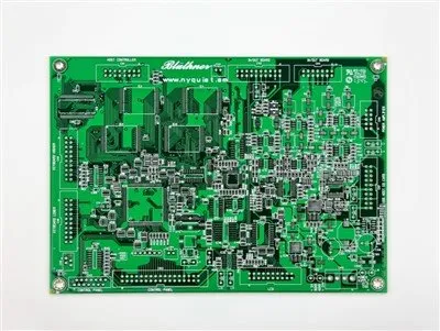
First off, let’s talk about miniaturization that’s not just “smaller for small’s sake.” A few years back, we were all excited about 0201 components (those tiny chips half the size of a grain of rice). Now? We’re sliding into 01005 parts, which are barely visible to the naked eye — and don’t even get me started on chip-scale packages (CSPs) that sit directly on the PCB like a second skin. But here’s the catch: miniaturization doesn’t mean cutting corners on quality. We’ve had to upgrade our pick-and-place machines to handle these tiny buggers with sub-10-micron precision. Last quarter, we had a client who makes medical wearables come to us because their old assembly shop couldn’t keep up with 01005 placement without defects. We swapped in our new high-precision machines, cut their defect rate by 40%, and they’ve been with us ever since. Another big mini trend is 3D interconnects — think of it as stacking PCBs like a sandwich with tiny solder bumps instead of wires. It’s perfect for high-density applications like 5G base stations, where every square millimeter matters. But let’s be real, this isn’t just our observation — I’ve chatted with other assembly peers at industry meets, and everyone’s scrambling to master 01005 and 3D stacks because clients are demanding smaller, lighter products without sacrificing performance.
Next up, smart manufacturing — but not the fancy, jargon-heavy “Industry 4.0” buzzword stuff. Wait, hear me out. We’re using real-time data now to fix problems before they happen. Our solder paste printers are hooked up to a dashboard that alerts us if the paste thickness is off by even 5 microns, or if a component is loaded incorrectly. No more waiting until the reflow oven step to find a defect — we catch it mid-process. Last month, a tech noticed a weird blip on the dashboard during a run for a client’s automotive sensor. It turned out the component tape was misaligned, so we fixed it before 200 boards went through reflow, saving the client thousands in rework. We also use AI-powered optical inspection (AOI) tools that don’t just look for cold solder joints — they spot patterns, like a certain brand of component that’s prone to shifting during placement, and adjust the machine’s pressure automatically. It’s not Skynet, it’s just… smart. And here’s the thing: clients love this because it means less downtime, faster turnaround, and fewer “oops, we messed up” moments. I’ve had so many buyers tell me they’re tired of assembly shops that treat every run the same — now, we tailor the process using that real-time data, which is a huge differentiator.
Then there’s the big push for sustainability — yes, even in PCB assembly. Let’s face it, electronics waste is a mess, and clients (especially in Europe and North America) are asking more about how we build their boards to be eco-friendly. We’ve swapped our leaded solder for lead-free alternatives that meet RoHS standards, but it’s more than that. We now recycle 95% of our process waste: scrap copper from PCB panels, unused solder paste, even the paper tape from component reels. We’ve also started offering “design for disassembly” (DfD) guidance for clients — tips on how to make their products easier to take apart later, so components can be reused instead of thrown away. A few months back, we worked with a consumer electronics startup that wanted their new Bluetooth speaker to be repairable. We adjusted our assembly process to use solder that’s easy to desolder, instead of super-melty high-temperature stuff, and added clear labels for each component. They launched it last month, and customers are raving about how easy it is to fix. Sustainability isn’t just a trend here — it’s non-negotiable now. Clients will pick an assembly shop with green practices over one that cuts corners on waste, even if it costs a tiny bit more.
Another emerging trend: specialized assembly for new tech sectors. We used to mostly work with consumer electronics and industrial clients. Now? We’re doing a ton of work for electric vehicles (EVs) and space tech. EV PCBs are built to withstand crazy temperature swings and high vibration — so we’ve had to update our reflow ovens to handle lead-free solder that sets stronger, and add vibration testing stations. Last year, we landed a job assembling PCBs for a small EV battery management system (BMS) maker. The BMS boards need to track 100+ battery cells at once, so we had to use high-density connectors that can handle high currents without overheating. We ran 500 thermal cycles on the boards to make sure they’d hold up in hot desert climates and cold mountain roads — and passed with flying colors. Space tech, though? That’s a whole other beast. The PCBs we build for CubeSats have to survive launch vibrations, radiation in space, and zero-gravity conditions. We use special materials for the PCB substrate, like aluminum nitride, that dissipate heat better, and conformal coatings that block radiation. It’s tricky, but it’s also super exciting — clients in space are pushing us to innovate, which makes us better at all types of assembly.
Wait, let’s not forget about supply chain resilience. Oh man, the chip shortage a couple years back really woke everyone up. Now, both our team and our clients are prioritizing component obsolescence planning. We keep a database of 10,000+ components and their end-of-life dates, so we can flag when a part is going out of production and work with clients to swap it out early — before it causes a delay. Last year, a client’s go-to microcontroller was discontinued, and we caught it 6 months before they needed to scale production. We found a pin-compatible alternative, tested it, and had them ready to switch without missing a deadline. We also work with local component suppliers now, instead of only overseas, to cut down on lead times. Sure, some parts still come from Asia, but having a local backup means we can get a critical component in 2 days instead of 2 weeks. Clients care a lot about this now — no one wants to delay a product launch because a part is backordered.
Now, let’s be honest — no trend is perfect. Miniaturization means we have to be way more careful with ESD (electrostatic discharge) — a single static shock can ruin an 01005 component. We added ESD mats on every workbench and trained our techs to wear wrist straps even when they’re not handling components directly. Smart manufacturing can have glitches — our AI AOI tool once flagged a good solder joint as defective because of a weird light reflection, so we had our engineers tweak the algorithm to account for that. Sustainability means lead-free solder is trickier to work with — it requires higher reflow temperatures, which can damage some components if we’re not careful. But that’s the fun part, right? We adapt.
At the end of the day, what all these trends boil down to is better for our clients. Smaller products, less waste, faster turnaround, more reliable tech — that’s what we’re here for. If you’re an engineer, product manager, or supply chain lead who’s tired of assembly shops that treat your project like just another run, let’s chat. We can walk through your design, talk about how to implement these trends for your specific product, and make sure you get a board that’s built right, on time, and at a price that makes sense. No generic pitches, no fine print — just straight talk about what works (and what doesn’t) for your project.
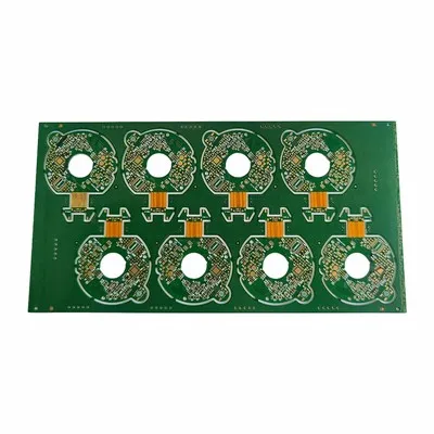
Rigid Flex PCB References:
- IPC Association Connecting Electronics Industries. (2023). "Trends in PCB Assembly Technology: Miniaturization and High-Density Interconnects"
- McKinsey & Company. (2024). "Sustainability in Electronics Manufacturing: Balancing Performance and Eco-Friendliness"
- Electronics Weekly. (2023). "Smart Manufacturing in PCB Assembly: Real-Time Data and AI Quality Control"
- Automotive News. (2024). "EV Electronics: Challenges in High-Reliability PCB Assembly for Vehicle Applications"
- Space News. (2023). "CubeSat PCBs: Materials and Processes for Space Environment Durability"
Huaswin Electronics Technology Co., Ltd.
Address: Building A2, Hao Hai Hong Industrial Park, No.3 Yu He Road, Gong He, Sha Jing, Bao An, Shenzhen
E-mail: sales@huaswin.com
WebSite: https://www.huaswin-pcba.com/
